The AMD 3rd Gen Ryzen Deep Dive Review 3700X and 3900X Raising The Bar AnandTech

403 Forbidden

Forbidden

You don't have permission to access /api.php

on this server.

Additionally, a 403 Forbidden

error was encountered while trying to use an ErrorDocument to handle the request.


L2
L3


8C
8C
6C
6C

is launching 5 different SKUs today, with the 16-core set to follow sometime in September. For today's launch sampled the R9 and R7 , and we took them for a ride in the limited time we had with them, covering as much as we could.

Starting at the top we have the Ryzen , which is a 12-core design. In fact it's the first 12-core processor in a standard desktop socket, and it rather unique within 's product stack because it is currently the only SKU which takes full advantage of ’s newest chiplet architecture. Whereas all the other Ryzen parts are comprised of two chiplets – the base I/O die and a single CPU chiplet – comes with two such CPU chiplets, granting it (some of) the extra cores and the 64MB of L3 cache that entails.

Interestingly, while has increased the core-count by 50% over its previous flagship processor, it has managed to keep the to the same as on the Ryzen 2700X. On top of this, the chip clocks in 300MHz faster than the predecessor in terms of boost clock, now reaching GHz; even the base clock has been increased by 100MHz, coming in at GHz. The big question then, is whether the new 7nm process node and Zen 2 are really this efficient, or should we be expecting more elevated power numbers?

Meanwhile our second chip of the day is the new Ryzen , which is configured and positioned as a particularly efficient model. With a boost clock of GHz and a base clock of GHz, the part should still be notably faster than the Ryzen 2700X, yet has managed to make this a part which is going to make for some interesting analysis.

Large Performance s, Particularly for Gaming

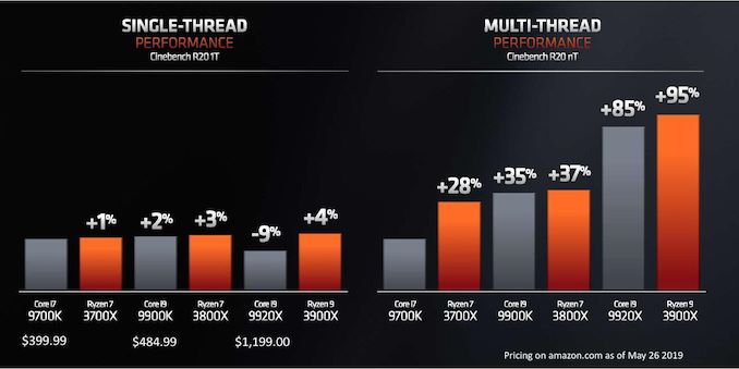
Positioning the Ryzen 3000 series against ’s line-up is a matter of both performance as well as price. had already made comparisons between the new SKUs and ’s counterparts back at Computex, where we saw comparisons between similarly priced units. According to the company, even 's pricey Skylake high-end desktop (HEDT) processor, the Core i9-9920X, isn't entirely out of the line of fire of the Ryzen .

Comparison: vs


/Threads
/ GHz /Turbo / 5.0 GHz
Lanes
(No Gen)
L2
4x 1
6 total
L3 1
(List)

Taking a look at chip pricing and positioning then, the big flagship fight among desktop processors is going to be between the Ryzen at , and the i9-9900K at . Both of which happen to be the highest-end SKUs of their respective mainstream desktop computing platforms.

Here should have a significant lead in terms of the multi-threaded performance of the new series as it’s able to employ 50% more cores than , all while promising to remain in a similar range of vs . We still expect the 9900K to win some workloads which are more lightly threaded simply due to ’s clock frequency lead, however this is something we’ll investigate more in detail in the coming benchmark analysis.

Comparison: vs


/Threads
/ GHz /Turbo / 4.9 GHz
Lanes
(No Gen)
L2
2x 1
L3
(List)

The is an interesting SKU. With only one populated CPU chiplet, the unit has half the available L3 cache versus the . But it also has all the CPU cores within its one chiplet active. In theory this does mean that the CPU cores have less overall L3 cache available to them, as they have to share it with an additional core within their respective CCXs.

With a GHz/Ghz base/boost clock configuration, we expect the to outperform the previous generation 2700X in all scenarios. The competition here based on pricing is the. again should have a single-threaded performance advantage thanks to its 500 MHz higher clocks – but we’ll have to see how both chips match up in daily workloads.

Zen 2 Microarchitecture Analysis: Ryzen 3000 and EPYC Rome

On the memory controller side particularly, promises a wholly revamped design that brings new support for a whole lot faster DDR4 modules, with the chip coming by default categorized as supporting DDR4-, which is a bump over the DDR- support of the Ryzen 2000 series.

had published an interesting slide in regards to the new faster DDR support that went well above the officially supported speeds, with claiming that the new controllers are able to support up to DDR4-4200 with ease and overclocking being possible to achieve ever higher speeds. However there’s a catch: in order to support DDR4 above , the chip will automatically change the memory controller to infinity fabric clock ratio from being 1:1 to 2:1.

Whilst this doesn’t bottleneck the bandwidth of the memory to the cores as the new microarchitecture has now doubled the bus width of the Infinity Fabric to 512 bits, it does add a notable amount of cycles to the overall memory latency, meaning for the very vast majority of workloads, you’re better off staying at or under DDR4- with a 1:1 MC:IF ratio. It’s to be noted that it’s still possible to maintain this 1:1 ratio by manually adjusting it at higher MC speeds, however stability of the system is no longer guaranteed as you’re effectively overclocking the Infinity Fabric as well in such a scenario.

The figures published on this page are run on DDR4-CL16 on the Ryzen and 2700X at timings of 16-16-16-36, and the i9-9900K was run with similar DDR4-CL16 at timings of 16-18-18-36.

Looking at the memory latency curves in a linear plotted graph, we see that there’s some larger obvious differences between the new Ryzen and the Ryzen 2700X. What immediately catches the eye when switching between the two results is the new 16MB L3 cache capacity which doubles upon the 8MB of Matisse. We have to remind ourselves that even though the whole chip contains 64MB of L3 cache, this is not a unified cache and a single CPU core will only see its own CCX’s L3 cache before going into main memory, which is in contrast to ’s L3 cache where all the cores have access to the full amount.

Before going into more details in the next graph, another thing that is obvious is that seemingly the ’s DRAM latency is a tad worse than the 2700X’s. Among the many test patterns here the one to note is the “Structural Estimate” curve. This curve is actually a simple subtraction of the TLB+CLR Thrash tests minus the TLB Penalty figure. In the former, we’re causing as much cache-line replacement pressure as possible by repeatedly hitting the same cacheline within each memory page, also repeatedly trying to miss the TLB. In the latter, we’re still hitting the TLB heavily, but always using a different cache-line and thus having a minimum of cache-line pressure, resulting in an estimate of the TLB penalty. Subtracting the latter from the former gives us a quite good estimate of the actual structural latency of the chip and memory.

Precisely when looking at the other various patterns in the graph, we’re seeing quite a large difference between the and the 2700X, with the showcasing notably lower latencies in a few of them. These figures are now a result of the new Zen2’s improved prefetchers which are able to better recognize patterns and pull out data from DRAM before the CPU core will handle that memory address.

In terms of the DRAM latency, it seems that the new Ryzen has regressed by around 10ns when compared to the 2700X (Note: Just take into the leading edge of the “Structural Estimate” figures as the better estimate) with ~74-75.5ns versus ~65.7ns.

It also looks like Zen2’s L3 cache has also gained a few cycles: A change from ~7.5ns at 4.3GHz to ~8.1ns at GHz would mean a regression from ~32 cycles to ~37 cycles. Such as change however was to be expected since doubling of the L3 cache structure has to come with some implementation compromises as there’s never just a free lunch. Zen2’s L3 cache latency is thus now about the same as ’s – while it was previously faster on Zen+.

Further interesting characteristics we see here is the increase of the capacity of the L2 TLB. This can be seen in the “TLB Penalty” curve, and the depth here corresponds to ’s published details of increasing the structure from 1536 pages to 2048 pages. It’s to be noted that the L3 capacity now exceeds the capacity of the TLB, meaning a single CPU core will have only the best access latencies to up to 8MB in the cache before starting to have to page-walk. A similar behaviour we see in the L2 cache where the L1 TLB capacity only covers 256KB of the cache before having to look up entries in the L2 TLB.

Another very interesting characteristic of ’s microarchitecture which contrasts ’s, is the fact that prefetchers into the L2 cache, while only does so for the nearest cache-line. Such a behaviour is a double-edged sword, on one hand ’s cores have can have better latencies to needed data, but on the other hand in the case of a unneeded prefetch, this put a lot more pressure on the L2 cache capacity, and could in effect counter-act some of the benefits of having double the capacity over ’s design.

Switching over to the memory bandwidth of the cache hierarchy, there’s one obvious new chance in the and Zen2: the inclusion of 256-bit wide datapaths. The new AGU and path changes mean that the core is able to now handle 256-bit AVX instruction once per cycle which is a doubling over the 128-bit datapaths of Zen and Zen+.

There’s an interesting juxtaposition between ’s L3 cache bandwidth and ’s: here has essentially as 60% advantage in bandwidth as the CCX’s L3 is much faster than ’s L3, when accessed by a single core. Particularly read-write modifications within a single cache-line (CLflip test) are significantly faster in both the L2 and L3 caches when compared to ’s core design.

Deeper into the DRAM regions, however we see that is still lagging behind when it comes to memory controller efficiency, so while the improves copy bandwidth from 19.2GB/s to 21GB/s, it still remains behind the 9900K’s 22.9GB/s. The store bandwidth (write bandwidth) to memory is also a tad lower on the parts as the reaches 1GB/s versus ’s 18GB/s.


One aspect that excels in is memory level parallelism. MLP is the ability for the CPU core to “park” memory accesses when they are missing the caches, and wait on them to return back later. In the above graph we see increasing number of random memory accesses depicted as the stacked lines, with the vertical axis showcasing the effective access speedup in relation to a single access.

Whilst both and ’s MLP ability in the L2 are somewhat the same and reach 12 – this is because we’re saturating the bandwidth of the cache in this region and we just can’t go any faster via more accesses. In the L3 region however we see big differences between the two: While starts off with around 20 accesses at the L3 with a 14-15x speedup, the TLBs and supporting core structures aren’t able to sustain this properly over the whole L3 as it’s having to access other L3 slices on the chip.

’s implementation however seems to be able to handle over 32 accesses with an extremely robust 23x speedup. This advantage actually continues on to the DRAM region where we still see speed-ups up to 32 accesses, while peaks at 16.

MLP ability is extremely important in order to be able to actually hide the various memory hierarchy latencies and to take full advantage of a CPU’s out-of-order execution abilities. ’s Zen cores here have seemingly the best microarchitecture in this regard, with only Apple’s mobile CPU cores having comparable characteristics. I think this was very much a conscious design choice of the microarchitecture as knew their overall SoC design and future chiplet architecture would have to deal with higher latencies, and did their best in order to minimise such a disadvantage.

So while the new Zen2 cores do seemingly have worse off latencies, possibly a combined factor of a faster memory controller (faster frequencies could have come at a cost of latency in the implementation), a larger L3 but with additional cycles, it doesn’t mean that memory sensitive workloads will see much of a regression. has been able to improve the core’s prefetchers, and average workload latency will be lower due to the doubled L3, and this is on top the core’s microarchitecture which seems to have outstandingly good MLP ability for whenever there is a cache miss, something to keep in mind as we investigate performance further.

One of the biggest additions to 's AM4 socket is the introduction of the interface. The new generation of motherboards marks the first consumer motherboard chipset to feature natively, which looks to offer users looking for even faster storage, and potentially better bandwidth for next-generation graphics cards over previous iterations of the current GPU architecture. We know that the Zen 2 processors have implemented the new TSMC 7nm manufacturing process with double the L3 cache compared with Zen 1. This new centrally focused IO chiplet is there regardless of the core count and uses the Infinity Fabric interconnect; the chipset uses four lanes to uplink and downlink to the CPU IO die.

Looking at a direct comparison between 's AM4 X series chipsets, the chipset adds lanes over the previous and 's reliance on . A big plus point to the new chipset is more support for with allowing motherboard manufacturers to play with 12 flexible lanes and implement features how they wish. This includes 8 x lanes, with two blocks of x4 to play with which vendors can add SATA, x1 slots, and even support for 3 x NVMe M.2 slots.

, and Chipset Comparison
Interface
Max PCH Lanes 24 24 24
8 2 2
8 8 8
GPU Config

/x8*


/x4


/x4
N N N
Chipset
Y Y Y
Y Y N


* Due to two different variations of the chipset, one with a 15 W and another with an 11 W , the extra power allows for more lanes, thus better GPU support overall. One example is the ASUS Pro WS -Ace model.
** Same reason as above, adding extra lanes to the chipset naturally increases power consumption.

One of the biggest changes in the chipset is within its architecture. The chipset is the first chipset its manufactured in-house using ASia's IP, whereas previously with the and chipsets, ASia developed and produced it based on its 55nm architecture. While going from at 6.8 W at maximum load, was improved upon in terms of power consumption to a lower of 4.8 W. For , this has increased massively to an 11 W on its consumer models, with a 15 W variant for its more professional and enterprise-focused models. The difference between the two variations aside from power consumption is that the 15 W chipset adds extra lanes which seemingly increases power consumption greatly when compared to previous focused chipsets.

Another major change due to the increased power consumption of the chipset when compared to and is the cooling required. All but one of the launched product stack features an actively cooled chipset heatsink which is needed due to the increased power draw when using due to the more complex implementation requirements over . While it is expected will work on improving the on future generations when using , it's forced manufacturers to implement more premium and more effective ways of keeping componentry on cooler. This also stretches to the power delivery as announced that a 16-core desktop Ryzen processor is set to launch later on in the year which means motherboard manufacturers need to implement better power deliveries, and better heatsinks capable of keeping the processors efficient.

Memory support has also been improved with a seemingly better IMC on the Ryzen 3000 line-up when compared against the Ryzen 2000 and 1000 series of Some motherboard vendors are advertising speeds of up to DDR4-4400 which until , was unheard of. also marks a jump up to DDR4- up from DDR4- on , and DDR4- on . As we investigated in our Memory Scaling piece back in2019, we found out that the Infinity Fabric Interconnect scales well with frequency, and it is something that we will be analyzing once we get the launch of out of the way, and potentially allow motherboard vendors to work on their infant firmware for 's new 7nm silicon.

)

One of the key points that have been a pain in the side of non- processors using Windows has been the optimizations and scheduler arrangements in the operating system. We’ve seen in the past how Windows has not been kind to non- microarchitecture layouts, such as ’s previous module design in Bulldozer, the Qualcomm hybrid CPU strategy with Windows on Snapdragon, and more recently with

Obviously has a close relationship with Microsoft when it comes down to identifying a non-regular core topology with a processor, and the two companies work towards ensuring that thread and memory assignments, absent of program driven direction, attempt to make the most out of the system. With the May 10th update to Windows, some additional features have been put in place to get the most out of the upcoming Zen 2 microarchitecture and Ryzen 3000 silicon layouts.

Thread expansion is where cores are placed as far away from each other as possible. In ’s case, this would mean a second thread spawning on a different chiplet, or a different core complex/CCX, as far away as possible. This allows the CPU to maintain high performance by not having regions of high power density, typically providing the best turbo performance across multiple threads.

Because of how modern software, and in particular video games, are now spawning multiple threads rather than relying on a single thread, and those threads need to talk to each other, is moving from a hybrid thread expansion technique to a thread grouping technique. This means that one CCX will fill up with threads before another CCX is even accessed. believes that despite the potential for high power density within a chiplet, while the other might be inactive, is still worth it for overall performance.

For Matisse, this should afford a nice improvement for limited thread scenarios, and on the face of the technology, gaming. It will be interesting to see how much of an affect this has on the upcoming EPYC Rome CPUs or future Threadripper designs. The single benchmark provided in its explanation was Rocket League at , which reported a +15% frame rate gain.

For any of our users familiar with our Skylake microarchitecture deep dive, you may remember that introduced that enabled the processor to adjust between different P-states more freely, as well as ramping from idle to load very quickly – from 100 ms to 40ms in the first version in Skylake, then down to 15 ms with Kaby Lake. It did this by handing P-state control back from the OS to the processor, which reacted based on instruction throughput and request. With Zen 2, is now enabling the same feature.

already has sufficiently more granularity in its frequency adjustments over , allowing for 25 MHz differences rather than 100 MHz differences, however enabling a faster ramp-to-load frequency jump is going to help when it comes to very burst-driven workloads, such as WebXPRT (’s favorite for this sort of demonstration). According to , the way that this has been implemented with Zen 2 will require BIOS updates as well as moving to the Windows May 10th update, but it will reduce frequency ramping from ~30 milliseconds on Zen to ~1-2 milliseconds on Zen 2. It should be noted that this is much faster than the numbers tends to provide.

The technical name for ’s implementation involves CPPC2, or Collaborative Power Performance Control 2, and ’s metrics state that this can increase burst workloads and also application loading. cites a +6% performance gain in application launch times using PCk10’s app launch sub-test.

Another aspect to Zen 2 is ’s approach to heightened security requirements of modern As has been reported, a good number of the recent array of side channel exploits do not affect processors, primarily because of how manages its TLB buffers that have always required additional security checks before most of this became an issue. Nonetheless, for the issues to which is vulnerable, it has implemented a full hardware-based security platform for them.

The change here comes for the Speculative Store Bypass, known as Spectre v4, which now has additional hardware to work in conjunction with the OS or virtual memory managers such as hypervisors in order to control. doesn’t expect any performance change from these updates. Newer issues such as Foreshadow and Zombieload do not affect

The Ryzen system was run in the same way as the rest of our article with DDR4-CL16, same as with the i9-9900K, whilst the Ryzen 2700X had DDR- with similar CL16 16-16-16-38 timings.

SPECint2006 Speed Estimated Scores

In terms of the int2006 benchmarks, the improvements of the new Zen2 based Ryzen is quite even across the board when compared to the Zen+ based Ryzen 2700X. We do note however somewhat larger performance increases in 403.gcc and 483.xalancbmk – it’s not immediately clear as to why as the benchmarks don’t have one particular characteristic that would fit Zen2’s design improvements, however I suspect it’s linked to the larger L3 cache.

It’s also interesting that although Ryzen posted worse memory latency results than the 2700X, it’s still able to outperform the latter in memory sensitive workloads such as 429.mcf, although the increases for 471.omnetpp is amongst the smallest in the suite.

However we still see that has an overall larger disadvantage to in these memory sensitive tests, as the 9900K has large advantages in 429.mcf, and posting a large lead in the very memory bandwidth intensive 462.libquantum, the two tests that put the most pressure on the caches and memory subsystem.

SPECfp2006(C/C++) Speed Estimated Scores

In the fp2006 benchmarks, we gain see some larger jumps on the part of the Ryzen , particularly in 482.sphinx3. These two tests along with 450.soplex are characterized by higher data cache misses, so Zen2’s 16MB L3 cache should definitely be part of the reason we see such larger jumps.

453.povray isn’t data heavy nor branch heavy, as it’s one of the more simple workloads in the suite. Here it’s mostly up to the execution backend throughput and the ability of the front-end to feed it fast enough that are the bottlenecks. So while the Ryzen provides a big boost over the 2700X, it’s still largely lagging behind the 9900K, a characteristic we’re also seeing in the similar execution bottlenecked 456.hmmer of the integer suite.

SPEC2006 Speed Estimated Total

Overall, the is 20.8% faster in the integer and floating point tests of the SPEC2006 suite, which corresponds to a 13% IPC increase, the metric that officially uses to promote the Zen2 microarchitectural increases.

SPECint2017 Rate-1 Estimated Scores

In the int2017 suite, we’re seeing similar performance differences and improvements, although this time around there’s a few workloads that are a bit more limited in terms of their performance boosts on the new Ryzen .

SPECfp2017 Rate-1 Estimated Scores

In the fp2017 suite, things are also quite even. Interesting enough here in particular is able to leapfrog ’s 9900K in a lot more workloads, sometimes winning in terms of absolute performance and sometimes losing.

SPEC2017 Rate-1 Estimated Total

As for the overall performance scores, the new Ryzen improves by 18.1% over the 2700X. Although closing the gap greatly, it’s just shy of actually beating the 9900K’s absolute single-threaded performance.

SPEC2017 Rate-1 Estimated Performance Per GHz

Normalising the scores for frequency, we see that has achieved something that the company hasn’t been able to claim in over 15 years: It has beat in terms of overall IPC. Overall here, the IPC improvements over Zen+ are 10.5%, which is a bit lower than the 13% figure for SPEC2006.

We already know about ’s new upcoming Sunny Cove microarchitecture which should undoubtedly be able to regain the IPC crown with relative ease, but the question for is if they’ll be able to still maintain the single-thread absolute performance crown and continue to see 5GHz or similar clock speeds with the new core design.

.

WebXPRT 3 (2018)

WebXPRT15

Speedometer 2

Google Octane 2.0

Mozilla Kraken 1.1

Overall, in the web tests, the new Ryzen and perform very well with both chips showcasing quite large improvements over the 2700X.

We’re seeing quite an interesting match-up against ’s 9700K here which is leading the all the benchmarks. The reason for this is that SKU has SMT turned off. The singe-threaded performance advantage of this is that the CPU core no longer has to share the µOP cache structure between to different threads, and has the whole capacity dedicated to one thread. Web workloads in particular are amongst the most instruction pressure heavy workloads out there, and they benefit extremely from turning SMT off on modern cores.

Whilst we didn’t have the time yet to test the new and with SMT off, ’s core and op cache works the same in that it’s sharing the capacity amongst two threads, statically partitioning it. I’m pretty sure we’d see larger increases in the web benchmarks when turning off SMT as well, and we’ll be sure to revisit this particular point in the future.

.

AppTimer: GIMP 2.10.4

(1 MB)

3D Particle Movement v2.1

3D Particle Movement v2.1 (with AVX)

Dolphin 5.0 Render Test

DigiCortex 1.20 (32k Neuron, 1.8B Synapse)

y-Cruncher 0.7.6 Single Thread, 250m Digitsy-Cruncher 0.7.6 Multi-Thread, 250m Digits

Agisoft Photoscan 1.3.3, Complex Test

.

Corona 1.3 mark


Luxk v3.1 C++Luxk v3.1 OpenCL

The Persistence of Vision ray tracing engine is another well-known benchmarking tool, which was in a state of relative hibernation until released its Zen processors, to which suddenly both and were submitting code to the main branch of the open source project. For our test, we use the built-in benchmark for all-cores, called from the command line.

POV-Ray 3.7.1 mark

.

Handbrake 1.1.0 - 60 x264 6000 kbps FastHandbrake 1.1.0 - 60 x264 3500 kbps FasterHandbrake 1.1.0 - 60 HEVC 3500 kbps Fast

7-Zip 1805 Compression7-Zip 1805 Decompression7-Zip 1805 Combined

WinRAR 5.60b3

AES Encoding

.

3Dk Physics - Ice Storm Unlimited3Dk Physics - Cloud Gate3Dk Physics - Fire Strike3Dk Physics - Time Spy3Dk Physics - Time Spy

The older Ice Storm test didn't much like the, pushing it back behind the R7 1800X. For the more modern tests focused on PCs, the 9900K wins out. The lack of HT is hurting the other two parts.

Geek4: Synthetics

A common tool for cross-platform testing between mobile, PC, and Mac, Geek 4 is an ultimate exercise in synthetic testing across a range of algorithms looking for peak throughput. Tests include encryption, compression, fast Fourier transform, memory operations, n-body physics, matrix operations, histogram manipulation, and HTML parsing.

Geekbench 4 - ST Overall

Geekbench 4 - MT Overall

(1 MB)

3DPM v1 Single Threaded3DPM v1 Multi-Threaded

x264 HD : Older Transcode Test

x264 HD Pass 1x264 HD Pass 2

Cine 11.5 and 10

Legacy: Cine 11.5 MultiThreadedLegacy: Cine 11.5 Single Threaded

error was encountered while trying to use an ErrorDocument to handle the request.

CPU Gaming 2019 List


ium

4K

.

111229.png

ium
111229.png 111231.png 111233.png 111235.png
111230.png 111232.png 111234.png 111236.png

error was encountered while trying to use an ErrorDocument to handle the request.

CPU Gaming 2019 List
 Ultra 4K 8K

.

111239.png

ium
111237.png 111239.png 111241.png 111243.png

error was encountered while trying to use an ErrorDocument to handle the request.

CPU Gaming 2019 List


4K

Ashes has dropdown options for MSAA, Light Quality, Object Quality, Shading Samples, Shadow Quality, Textures, and separate options for the terrain. There are several presents, from Very to Extreme: we run our benchmarks at the above settings, and take the frame-time output for our average and percentile numbers.

.

111255.png

ium
111253.png 111255.png 111257.png 111259.png
111254.png 111256.png 111258.png 111260.png

Strange Brigade is based in 1903’s Egypt and follows a story which is very similar to that of the Mummy film franchise. This particular third-person shooter is developed by Rebellion Developments which is more widely known for games such as the Sniper Elite and Alien vs Predator series. The game follows the hunt for Seteki the Witch Queen who has arose once again and the only ‘troop’ who can ultimately stop her. play is cooperative centric with a wide variety of different levels and many puzzles which need solving by the British colonial Secret Service agents sent to put an end to her reign of barbaric and brutality.

The game supports both the DirectX 12 and s and houses its own built-in benchmark which offers various options up for customization including textures, anti-aliasing, reflections, draw distance and even allows users to enable or disable motion blur, ambient occlusion and tessellation among others. has boasted previously that Strange Brigade is part of its implementation offering scalability for multi-graphics card configurations.

error was encountered while trying to use an ErrorDocument to handle the request.

CPU Gaming 2019 List


ium

4K
*Strange Brigade is run in and modes

.

111263.png

Strange Brigade ium
111261.png 111263.png 111265.png 111267.png
111262.png 111264.png 111266.png 111268.png

111271.png

Strange Brigade ium
111269.png 111271.png 111273.png 111275.png
111270.png 111272.png 111274.png 111276.png

The highly anticipated iteration of the Grand Theft Auto franchise hit the shelves on il 14th, with both and NVIDIA in tow to help optimize the title. GTA doesn’t provide graphical presets, but opens up the options to users and extends the boundaries by pushing even the hardest systems to the limit using Rockstar’s Advanced Engine under DirectX 11. Whether the user is flying high in the mountains with long draw distances or dealing with assorted trash in the city, when cranked up to maximum it creates stunning visuals but hard work for both the CPU and the GPU.

error was encountered while trying to use an ErrorDocument to handle the request.

CPU Gaming 2019 List


Very
4K
*Strange Brigade is run in and modes

There are no presets for the graphics options on GTA, allowing the user to adjust options such as population density and distance scaling on sliders, but others such as texture/shadow/shader/water quality from to Very . Other options include MSAA, soft shadows, post effects, shadow resolution and extended draw distance options. There is a handy option at the top which shows how much video memory the options are expected to consume, with obvious repercussions if a user requests more video memory than is present on the card (although there’s no obvious indication if you have a low end GPU with lots of GPU memory, like an R7 240 4GB).

.

111279.png

ium
111277.png 111279.png 111281.png 111283.png
111278.png 111280.png 111282.png 111284.png

Aside from keeping up-to-date on the Formula One world, F12019 added HDR support, which F1 has maintained; otherwise, we should see any newer versions of Codemasters' EGO engine find its way into F1. Graphically demanding in its own right, F1 keeps a useful racing-type graphics workload in our benchmarks.

Aside from keeping up-to-date on the Formula One world, F12019 added HDR support, which F1 has maintained. We use the in-game benchmark, set to run on the Montreal track in the wet, driving as Lewis Hamilton from last place on the grid. Data is taken over a one-lap race.

error was encountered while trying to use an ErrorDocument to handle the request.

CPU Gaming 2019 List
F1


4K
4K

.

111287.png

F1 ium
111285.png 111287.png 111289.png 111291.png
111286.png 111288.png 111290.png 111292.png

Power consumption of the new Ryzen 3900 and are of particular interest because it’s a very key aspect of the new generation chipsets, and promises some extremely large improvements thanks to the new 7nm process node as well as the optimised chiplet design.

When comparing the single-chiplet Ryzen to the previous generation Ryzen 2700X, we’re seeing quite some dramatic differences in core power consumption. In particular power consumption at each chip’s respective peak frequency is notably different: Although the new has a 100MHz higher clock speed and thus is further up the exponential power curve, it manages to showcase 32% lower absolute power than the 2700X.

We have to remember that we’re talking about overall absolute power, and not efficiency of the chip. When taking actual performance into account through the higher clock as well as Zen2’s increased performance per clock, the Performance/W figures for the new should be significantly higher than its predecessor.

    • 88W for 142W for
    • 60A for 95A for
  • : the maximum amount of current at any instantaneous short period of time that can be delivered by the motherboard’s voltage regulators.
    • 90A for 140A for

Looking at the total power consumption of the new , the chip is very much seemingly hitting and maintaining the 88W PPT limitations of the default settings, and we’re measuring 90W peak consumption across the package.

When having a closer look at the new , first we have to enjoy the sheer amount of cores of this processor!

Following that, we see that this CPU’s per-core peak power consumption is quite notably higher than that of the , which is not a surprise given that the chip is clocked 200MHz higher at GHz versus “just” GHz. However even at this much higher clock, the ’s power consumption remains notably lower than that of the 2700X.

Scaling up in threads as well as cores, we’re seeing a similar scaling behaviour, with the large difference being that the is maintaining higher power consumption per core (and frequency) than the . Fully loading the chip we’re seeing 118W power on the CPU cores while the package power is falling in at the exact 142W that describes as the PPT limit of processors such as the .

Another thing to note in the results between the results and the , is that un-core power on the latter is quite higher. This really shouldn’t come as a surprise as the processor has a second chiplet who will have L3 and Infinity Fabric that will use more power.

Graphing the three processors together, we see two main aspects: Again the and both consuming notably less power than the 2700X, and the ’s hard limit when reaching the 88W PPT limit while the is able to scale further up till it hits the 142W limit.

Power (Package), Full Load

Comparing the full load power characteristics of both SKUs, they end up extremely competitive in both their respective categories. The ’s 90W hard-limit puts it at the very bottom of the CPUs we’ve used in our testing today, which is quite astonishing as the chip is trading blows with the 9700K and 9900K across all of our test workloads, and the latter chip’s power consumption is well over 60% above the ’s.

The is also impressive given that it’s a 12-core CPU. While posting substantial performance improvements of the 12-core Threadripper counterparts, the still manages to be significantly less thermally constrained thanks to its much lower power consumption, peaking in at 142W.

The most interesting aspect of ’s new opportunistic power boost mechanism lies in a CPU we weren’t able to test today: the . At stock behaviour, the chip’s should allow it to behave a lot more like the when it comes to the higher thread-count frequencies, at least until it maxes out its 8 cores on its single chiplet, which might really put it ahead of the in terms of multi-threaded performance workloads.

POV-Ray 3.7.1 mark (Overclocking)

In POV-Ray, running the at a flat 4.3GHz gives it a 8.2% performance boost over stock. Enabling PBO doesn’t make much difference in multi-threaded workloads for the as it’s still being limited by the 142W PPT limit.

Unfortunately we weren’t able to further investigate raising the PPT limit for this article due to time contraints as well as currently non-final firmware version for motherboards from the vendors.

Cinebench R15 Single Threaded (Overclocking)

Turning on PBO will increase the single-threaded performance of the by a few percent, scoring just slightly higher than the stock settings. Naturally the 4.3 GHz flat overclock will regress in performance as it loses out 300MHz peak frequency compared to stock.

Cinebench R15 Multi-Threaded (Overclocking)

Overall, we’ve been eagerly awaiting today’s launch for months, and all the while has certainly given us some high expectations for their 3rd generation Ryzen CPUs. At the end of the day I think that was able to deliver on all of their promises, and hitting all of the performance targets that they needed to. Furthermore, where kills it is in terms of value, as both the and the really deliver in terms of offering outstanding alternatives to the competition.

The basis for the new 3rd generation Ryzen processors is ’s new high-risk high-reward bet on moving away from a single monolithic die to a chiplet-based MCM (Multi-chip module) design. What this has allowed to do is to maximise the performance characteristics of their 7nm design for the new Ryzen 3000 chipsets. Meanwhile, having the I/O components and the memory controllers on a 12nm process node not only allows to minimise the cost of the platform, but also allows them to optimise the silicon for their specific use-cases.

The actual CPU chiplets (CPU-lets?) are manufactured on TSMC’s leading edge 7nm process node and has seemingly been able to take full advantage of the process, not only lowering the power consumption of the cores, but actually also raising the clock frequency at the same time, bringing for some impressive power efficiency benefits.

The new design did seemingly make some compromises, and we saw that the DRAM memory latency of this new system architecture is slower than the previous monolithic implementation. However, here is also where things get interesting. Even though this is a theoretical regression on paper, when it comes to actual performance in workloads the regression is essentially non-existent, and is able to showcase improvements even in the most memory-sensitive workloads. thanks to the new Zen 2 CPU core’s improved microarchitecture, with new improved prefetchers and overall outstanding Memory Level Parallelism (MLP) designs. Further helping 's memory/cache situation is the doubling of the CCX’s L3 cache from 8MB to 16MB, which on average, ends up with better workload memory performance.

In the majority of controlled tests, has done something they haven’t been able to achieve in almost 15 years, since the tail-end of the Athlon 64's reign in 2005: that is to have a CPU microarchitecture with higher performance per clock than 's leading architecture. Zen 2 finally achieves this symbolic mark by a hair’s margin, with the new core improving IPC by 10-13% when compared to Zen+.

Having said that, still very much holds the single-threaded performance crown by a few percent. ’s higher achieved frequencies as well as continued larger lead in memory sensitive workloads are still goals that has to work towards to, and future Zen iterations will have to further improve in order to have a shot at the ST performance crown.

Beyond this, it’s remarkable that has been able to achieve all of this while having significantly lower power consumption than 's best desktop chip, all thanks to the new process node.

The & Versus The Competition, Verdict

It’s in these categories where ’s strengths lie: In the majority of our systems benchmarks, more often than not is able to lead ’s 9700K and 9900K in terms of performance. Particularly it was interesting to see the new 3rd gen Ryzens post larger improvements in the web tests, all thanks to Zen 2’s improved and larger op cache.

In anything that is remotely multi-threaded, is also able to take the performance crown, with only ’s HEDT i9-7920X being able to top the new 12-core Ryzen . The here still hangs in there being extremely competitive, falling in-between the 9700K and 9900K when it comes to multi-threaded workloads, sometimes even beating the 9900K in some workloads, a respectable result.

That being said, the new and are posting enormous improvements over the 2700X, and we can confirm ’s claims of up to 30-35% better performance in some games over the 2700X.

Here’s the thing: while does still lag behind in gaming performance, the gap has narrowed immensely to the point that the Ryzen CPUs are no longer something to be dismissed if you want to have a high-end gaming machine, and are still very much a viable option worth considering.

Everything Tied Together: A Win For

What really does make the Ryzen and winners in my eyes is their overall packages and performance. They’re outstanding all-rounders and has managed to vastly improve some of the aspects it was lagging behind the most. Whilst has to further push single-threaded performance in the future and continue working on improving memory performance, they’re on ’s tail.

The big argument for the and is their value as well as their power efficiency. At the particularly seems exciting and posts near the same gaming performance as the at . Considering that is also shipping the CPU with a viable Wrath Spire, this also adds on to the value that you get if you’re budget conscious.

The essentially has no competition when it comes to the multi-threaded performance that it’s able to deliver. Here the chip not only bests ’s designs, which is able to go toe-to-toe only with >$1500  HEDT platforms, but also suddenly makes ’s own Threadripper line-up quite irrelevant.

All in all, while still has some ways to go, they’ve never been this close to in over a decade, and if the company is able to continue to execute as well, we should be seeing exciting things in the future.


0 Response to "The AMD 3rd Gen Ryzen Deep Dive Review 3700X and 3900X Raising The Bar AnandTech"

Post a Comment

Iklan Atas Artikel

Iklan Tengah Artikel 1

Iklan Tengah Artikel 2

Iklan Bawah Artikel